
The Missing 2x: Why Int8 is Twice as Fast as BF16
From bf16 to int8 subword parallelism

Have you ever looked at an ML accelerator spec sheet and noticed that peak OPs/s at int8 are exactly 2x higher than at bf16? But why? Is it just the type size difference? If it were just about storage, wouldn’t it be more useful to support fp8 instead?
| Accelerator | Peak bf16 (TFLOPs/s) | Peak int8 (TOPs/s) |
|-------------|----------------------|--------------------|
| TPU v6e     |                  918 |               1836 |
| TPU v5e     |                  197 |                393 |
| B200.       |                 5000 |              10000 |
And why do older chips, like TPU v4, offer identical throughput at int8 and bf16?
By the end of this article, we’ll cover:
What systolic arrays are
How the bf16 format works
How a bf16 processing element is implemented
How to extend it to support int8
How to achieve 2x throughput
This article reuses animations from my YouTube video covering the same topic. The article goes into much more depth, but do let me know what you think about the video format! It’s something I want to play around with more in the future.
Systolic Arrays
It would be an understatement to say that matrix multiplication is hard to optimize on traditional processors. I took a shot at CPU matmul optimizations in a previous article and it’s a good chunk of work to get even within a stone’s throw of reference implementations.
But fret not, throwing hardware at the problem is always an option and matmul is no exception. Systolic arrays are a particular type of circuit designed to achieve theoretically optimal arithmetic intensity (~do maximum amount of work per memory access) [1].
Take a look at the animation below to see a 4x4 weight-stationary systolic array in action. TPUs can have multiple systolic arrays per chip, each up to 256x256 in size.
Weight-stationary refers to how weights are loaded into the systolic array. Unlike the streamed activations, weights are loaded via double buffering. This significantly reduces the amount of data needing to be transferred between PEs every cycle.
bfloat16 format
Each cell in the systolic array, a so-called processing element, does one simple operation: a multiply-accumulate—the innermost body of the matrix multiplication code below:
for (int i = 0; i < N; ++i) {
  for (int j = 0; j < M; ++j) {
    for (int k = 0; j < K; ++k) {
      c[i][j] = a[i][k] * b[k][j] + c[i][j];
    }
  }
}
Below is an illustrated execution of the processing element.
bfloat16 format
To bridge the software-hardware gap, we need to understand how floats, particularly bf16 in our case, are encoded in bit form. I’ll assume you are familiar with how unsigned integers are encoded (if not, just nod along and trust the math).
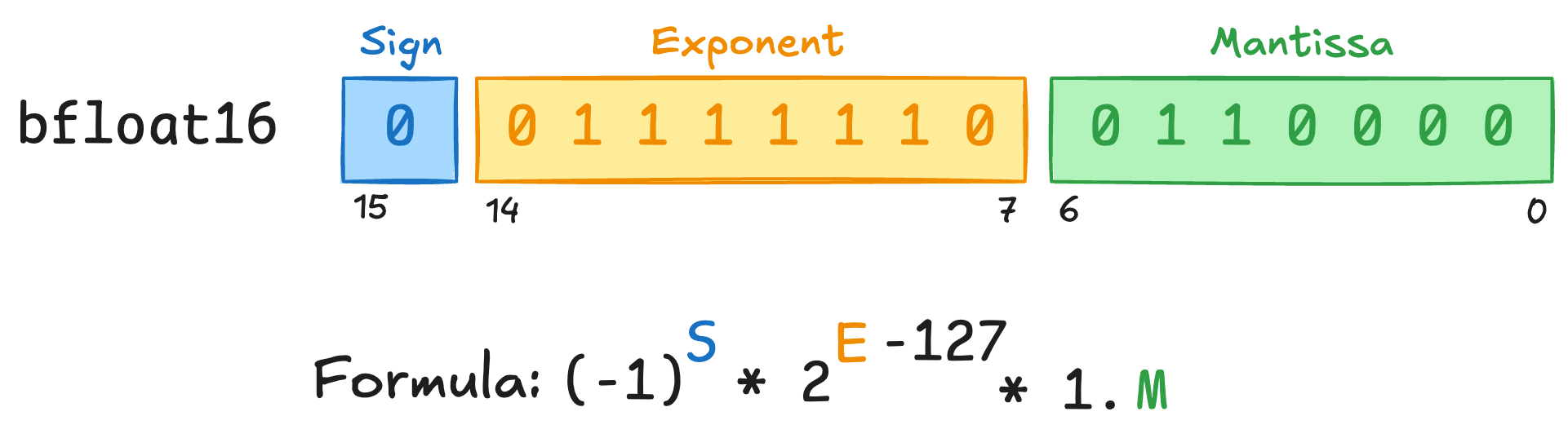
Figure 1 illustrates the bf16 format. It has 3 parts: a sign bit, 8 exponent bits, and 7 mantissa bits. Let’s tackle these 1 by 1.
Sign
The sign bit is simple: 0 depicts a positive number, 1 a negative number.
Exponent
In the formula above in figure 1, notice how the exponent is interpreted as an unsigned integer from which a bias is subtracted and the result is used to exponentiate the number 2. While somewhat arbitrary at first glance, let’s work through this.
The range of possible exponents is between -126 to +127, using up 254 of the 256 total possible values. The remaining values are used for special states like NaN and INF. We’ll ignore the existence of these states (a luxury hardware engineers don't have), but it’s worth highlighting that they exist and the hardware must correctly handle them.
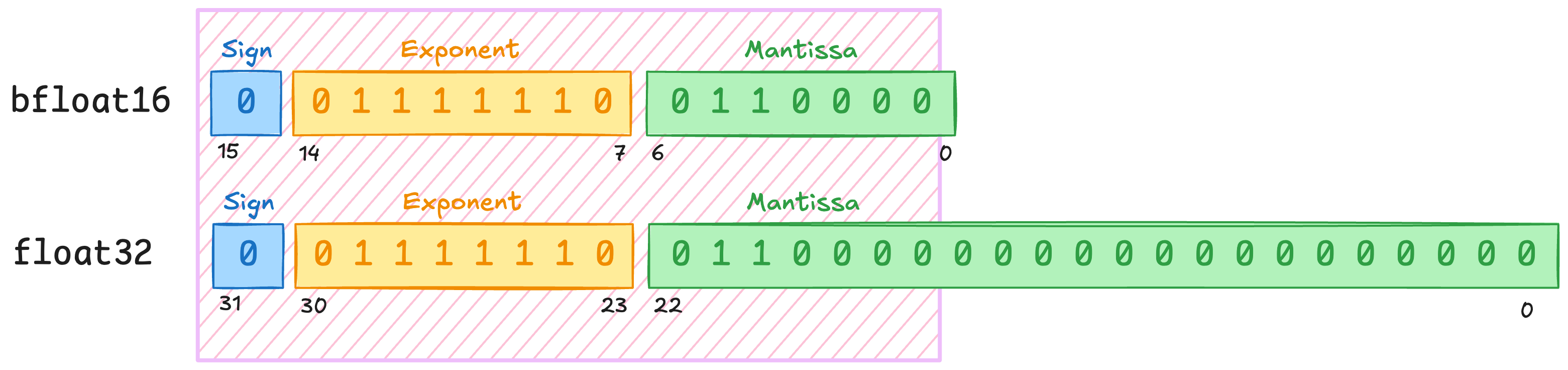
It’s also worth highlighting that single precision floats (fp32) use exactly the same exponent encoding and number of bits.
Mantissa
The mantissa represents a fractional number in the interval [1, 2). This is achieved by having 7 variable bits and an implicit 8th most-significant bit always set to 1. If we interpret this as an integer, it gives us a range from 128 to 255. To get to the fractional number, we can divide by 128.
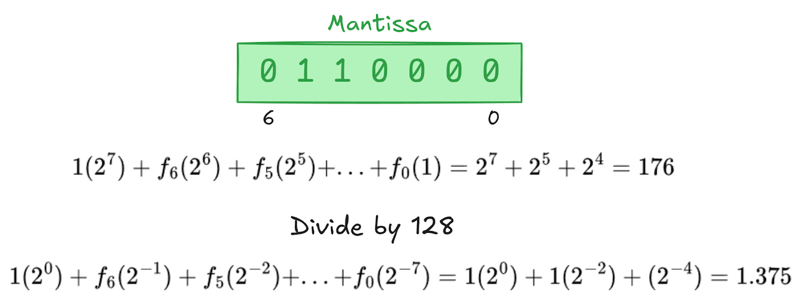
The Mantissa Invariant: Because of the implicit leading 1, the mantissa always represents a value in the interval [1, 2). Keep this rule in mind—it is going to cause us a minor headache once we tackle multiplication.
Encoding float into bf16 format
Since the above feels a bit reversed - it tells one how to read a bf16 number not how to encode one - take a look at the animation below showing how to marshall a float into the binary format.
bfloat16 multiplication
Now that we understand how bf16 is represented, let’s see how to multiply two bf16 numbers. Figure 3 shows something interesting: algebraically we can determine the sign, exponent, and mantissa independently of each other. Let’s see how to implement this in hardware.

Sign
The resulting sign can be determined with an XOR.
| A | B | XOR |
|---|---|-----|
| 0 | 0 |   0 |
| 0 | 1 |   1 |
| 1 | 0 |   1 |
| 1 | 1 |   0 |
Exponent
Like we saw in Figure 3, multiplying two numbers of the form 2^x and 2^y is the same as adding their exponents 2^{x+y}. But remember, the 8-bit values stored in the hardware (let's call them E_A and E_B) are biased. The actual mathematical values we are multiplying are:
We need to store this new product back into the bf16 format. This means the hardware must compute a new stored exponent, E_result, which will also have a single bias of 127 implicitly subtracted from it during decoding:
If we solve for the value the hardware actually needs to store (E_result), we get:
This is great news! To compute the new exponent, the circuit just naively adds the two 8-bit unsigned integers together and subtracts 127. This can be implemented extremely efficiently using standard integer adders.
Mantissa
Earlier, we saw that the mantissa is of the form 1.M, where M is 7 bits. Logically, this is equivalent to an 8-bit integer implicitly divided by 128.
We also established the mantissa invariant: the value must always stay in the interval [1, 2).
If we multiply two mantissas together, we’ll get a 16-bit product that can fall anywhere in the range [1, 4). That breaks the invariant! Let’s see this in action using good ol’ long multiplication.
If the product happens to be 2 or greater, it breaks our invariant! To re-establish it, the hardware has to check the result. If the product overflowed into the [2, 4) range, the circuit divides the mantissa by 2 (a simple bitwise right-shift) and compensates by adding 1 to the exponent. A proper implementation would have to check if this +1 causes an exponent overflow, but we will happily sweep that under the rug to protect our sanity.
After normalization, the next thing we need to discuss is the number of bits. Since we’ve established the invariant, we have 15 bits and the MSB is guaranteed to be 1, so we can treat it as the leading implicit 1 bit. That leaves us with 14 variable bits which, if I count right, is 7 more than we fit into a bf16 mantissa. This leaves us with 2 options:
Round down to bf16
Stay in higher precision
It might be tempting to go with choice one, but let’s think back - these multiplications happen in huge systolic arrays. Rounding errors can quickly accumulate and become catastrophic at that scale.
If particularly curious, try to write a script to simulate the rounding losses. Does it match your intuition?
Instead, it’s common to keep the bf16-bf16 product in fp32. That provides enough breathing room and as seen in figure 3, the only difference between bf16 and fp32 is the number of mantissa bits, making promotion trivial.
Let’s see bf16 multiplication end-to-end in the circuit form.
Addition
So we’ve multiplied two bf16 numbers and produced fp32 product. Now we need to add it to the fp32 partial result coming from the PE above.
We don't need to dive too deep into addition, but the key takeaway is that float addition requires a lot of circuitry to align decimal places before the actual math can commence. Watch the video below and notice how the circuit might have to shift numbers twice: once during initial alignment and then later to fix mantissa invariant if leading 1s get canceled out.
These shifters are expensive! In my local implementations synthesized with yosys, the 8x8 multiplier from earlier (with support for signed and unsigned integers) costs ~680 NAND2 gate equivalents, whereas the two shifters cost combined 760 NAND2 gates.
This is a notable difference from fp32 PEs and a big part of the reason that bf16 is preferred. In fp32 the cost is dominated by the multiplier unit since its footprint scales quadratically with the number of mantissa bits. Addition, on the other hand, is dominated by the alignment shifters [2].
Supporting int8
So far we have a PE that supports bf16 - that’s very cool, but what about int8? Out of the box we don’t get support and we need to do a little extra work.
Obviously, we could just extend the PE with dedicated int8 multiplication logic, dedicated int8 addition logic, and call it a day. That would work but chips don’t grow on trees so let’s try to be a little more economical.
int8 multiplication
You might’ve already noticed earlier - we already have an 8x8 multiplier for mantissa multiplication! Mantissas are unsigned whereas for int8 support we’d like to also have signed multiplication, but this is doable. One approach (and I’m not sure if it’s the one actually used in production PEs) is to use 9x9 signed multiplier.
Let’s see why this works:
uint8 can be promoted to int9 by adding a leading 0 bit (positive)
positive int8 can be promoted identically
negative int8 is a little nuanced, but it just requires copying the leading bit (sign extension)
Let’s walk through the last case using -5 as an example. In two's complement, the most significant bit acts as a negative weight:
# Two's complement -5
1111_1011 = -128 + 64 + 32 + 16 + 8 + 2 + 1 = -5
# Promoting to int9
1_1111_1011 = (-256 + 128) + 64 + 32 + 16 + 8 + 2 + 1 = -5
Notice how after the promotion, the math automagically balances out! The first two bits (-256 + 128) collapse right back into the -128 we started with.
My understanding is that since we aren’t actually using the full range of possible int9 products, the synthesized multiplier can prune some logic. We also don’t need the rest of the bf16 multiplication logic, so those can be completely disabled in int8 mode as shown in the video below.
Notice how we end up with a 16-bit integer product, which we can fit into the bottom half of the fp32 register.
Addition
In int8 mode, the partial sums are stored in int32 and the product is an int16. We simply bypass the fp32 addition logic completely (no longer needing the complex shifters) and add a dedicated adder.
Adders are much cheaper and since the int8 path is completely exclusive with the bf16 path, there’s likely quite a bit of slack even in a heavily pipelined implementation. An optimized implementation would take advantage of this slack to reduce the required chip area for the adder.
Have we done it?
Have we achieved 2x throughput? Sadly, not yet. However, this is basically what older TPUs up to v4 did [3].
Let’s see why exactly this achieves identical peak throughput as bf16 and use it as an opportunity to briefly discuss three concepts:
Clock frequency
Critical path
Pipelining
Clock frequency and critical path
The animation below illustrates the concepts of clock frequency and critical path. Notice how signal leaves the input registers on positive clock edge and has to propagate to the output registers before the next positive clock edge.
If the clock frequency is too high for the circuit, the signal doesn’t have time to settle into the output register. It’s common to have paths that are less complex but are required to operate at the global clock cycle speed determined by the critical path.
If we relate this back to bf16 and int8 paths, in the current implementation it’s likely the shifters that lie on the critical path. The int8 logic is much simpler, but is forced to operate at the same clock speed.
Pipelining
As we’ve seen, critical path is what limits the chip’s clock frequency. There are two ways forward:
Optimize critical path’s logic
Insert new registers into the critical path.
Optimizing the critical path might require divine intervention and even then there might be limitations. Let’s take a look at option 2, commonly known as pipelining.
In the animation below, the bf16 path uses a 4-stage pipeline, whereas the int8 path uses only 2 stages. To be honest, I’m not sure what is common in production chips - either would work with some extra accounting needed for cycle-by-cycle differences between bf16 modes and int8 modes.
While watching the video, notice even though the latencies are different, the throughput at saturation is exactly the same. This drives home the idea that int8 mode on its own doesn’t provide extra throughput.
Subword parallelism
We are on the final stretch, let’s keep pushing through.
So, how can we increase throughput to 2x? The obvious next thing to look at is that we are underutilizing our input wires by only using the bottom 8 bits in int8 mode. We can pack another int8 number there, the question remains which one?
Try to see if you can figure the answer out on your own before watching the animation below.
I suspect you see where this is going. We pack two neighboring (with respect to the dot product) int8s into a single PE. This technique—formally known as subword parallelism [5]—has actually been around since the 90s for multimedia acceleration. By applying it here, we just need the PE to do the elementwise multiplications in parallel and accumulate them. To do this, we need to add two things: a second 8x8 multiplier and a 3-way adder (to simultaneously sum product A, product B, and the incoming partial sum from the PE above).
The following animation illustrates the required changes.
This is pretty much exactly as one would expect, no surprises. Let’s talk briefly about the fact that we combine the two partial products into a single int32 accumulator. Since this operation is repeated many times, there’s a good question to ask: can it overflow?
Let’s take the worst-case: the largest possible product by the 8x8 multipliers is (-128) x (-128) = 16,384, which easily fits into int16. With subword parallelism, this doubles. Int32 has a max_val of 2^31 - 1, meaning we could repeat this operation 65k times before we have to worry about overflows.
Even if the systolic array was tiling over massive contracting dimension K, it would require K > 130k to even reach the possibility of overflow while assuming the absolute worst scenario. In practice, some products will be positive, some negative, so these largely cancel out. Suffice to say, this will never overflow, but good to sanity check it.
Cost
We’ve finally achieved 2x throughput. As we’ve seen before, the 8x8 multiplier cost around 700 NAND2 gates, so the total multiplier cost doubles.
In my functional, but not particularly optimized, SystemVerilog implementations, adding support for subword parallelism increases the cost in terms of NAND2 gates by a little over 20%. Considering that it gives us 2x throughput that seems like a no-brainer and is exactly why int8 subword parallelism is so commonly supported on modern systolic arrays.
Summary
We’ve covered a lot! We’ve seen:
what systolic arrays are
what processing elements do
how bf16 format works
how mantissa multipliers can be reused for int8 multiplication
how clock cycle, critical path, and pipelining are used
how subword parallelism achieves 2x throughput
And crucially, we’ve answered the question we started with: why TPU v4 doesn't offer a 2x throughput increase at int8, and why newer chips do.
References
[1] H. T. Kung, "Why Systolic Architectures?," Computer, vol. 15, no. 1, pp. 37-46, Jan. 1982.
[2] J. L. Hennessy and D. A. Patterson, Computer Architecture: A Quantitative Approach, 6th ed. Cambridge, MA, USA: Morgan Kaufmann, 2017. (Appendix J)
[3] N. P. Jouppi et al., "TPU v4: An Optically Reconfigurable Supercomputer for Machine Learning with Hardware Support for Embeddings," Proc. ACM/IEEE 50th Annu. Int. Symp. Comput. Archit. (ISCA), 2023.
[4] R. B. Lee, "Subword Parallelism with MAX-2," IEEE Micro, vol. 16, no. 4, pp. 51-59, Aug. 1996.
A Note from Michal
Hardware architecture can get pretty heavy, so my goal was to keep this as approachable as possible. I hope you learned something new about how ML chips tick and enjoyed the animations along the way! For me, understanding how the chips I work with on a daily basis work under the hood is super rewarding!
Enjoyed this article?
Subscribe to the Substack: If you haven’t already, consider subscribing!
Check out Animated Compute: Content for this article is entirely based on the research I did for my latest YouTube video. I’m planning to post more videos and work on improving the production quality, so I hope you’ll subscribe :)
After a well-deserved break for reading this far, perhaps check out some of my older articles.
Optimizing matrix multiplication

This article is all about performance optimizations - squeezing as much performance out of my CPU as I can.
GPU Programming

One of the great joys of software engineering is dispelling magic. I’ve written code that executed on a GPU using frameworks like PyTorch or TensorFlow, but I never understood the “how”. It’s time to dispel the magic of GPU programming and learn how it works under the hood.
How does SQLite store data?

Recently I’ve been implementing a subset of SQLite (the world’s most used database, btw) from scratch in Go. I’ll share what I’ve learned about how SQLite stores data on disk which will help us understand key database concepts. Thanks for reading Michal’s Substack! Subscribe for free to receive new posts and support my work.
Great visualizations. Particularly loved the first, showing matrix multiplication.
Oh, this is wonderful. I had figured out the v4 approach myself in the past, but didn't understand the missing piece for how v5 obtained 2x throughput. The gate cost estimate is instructive.